|
|
S. Sundar Kumar Iyer Office location: WL
122 Email: sskiyer [AT] iitk.ac.in I am also a part of the National Centre for Flexible
Electronics (FlexE Centre) which forms a bridge between academia and industry with
a goal of creating an eco-system for flexible electronic manufacturing in
India. It operates under the Samtel Centre
for Display Technologies at IIT Kanpur. |
Research and Development Interests
o
Organic Solar Cells
o
Flexible Photovoltaic Technology
o
Flexible Electronics
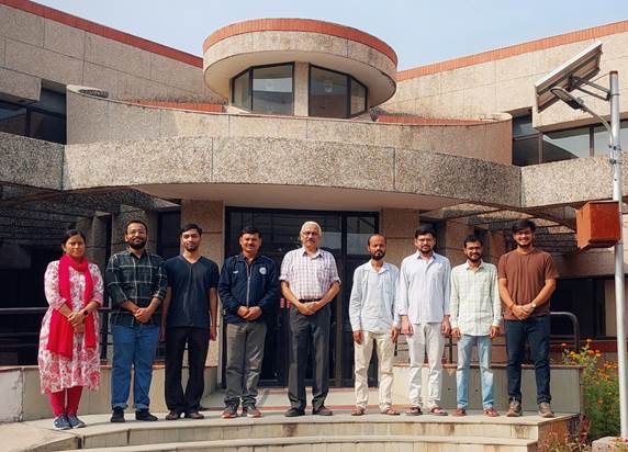
The FlexPV Team at IIT Kanpur
Photograph taken in front of Samtel Centre for Display Technologies on 15th November,
2023.
Technologies Developed
o
Organic photovoltaic solar
modules on glass substrate (Supported by MNRE, Govt. of India)
o
Organic solar modules on paper
substrate (Supported by MeitY, Govt. of India)
In the Press
o
International
Edition and Indian
Edition of pv magazine about the OPV modules built on paper substrates (29th
September, 2020)
o
Interview
in the The Electronics on
Flexible Electronics on the occasion of launching of Innovation Challenge
at the FlexE Centre, IIT Kanpur (12th
February, 2021)
Recent
Publications
o Guest Editorial
Special Issue on Flexible Electronics for Emerging Markets and Developing
Economies,
S. Sundar Kumar Iyer, et al., IEEE Journal on Flexible Electronics, Volume
2, Number 5, September 2023, pp. 333-335.
o Shelf-life
Comparison of Paper Solar Cells with either MoO3 or Epoxy as
Encapsulation Layers, Sambathkumar Balasubramanian, Eswaran Jayaraman
and S. Sundar Kumar Iyer, IEEE JFLEX, IEEE Journal on Flexible Electronics,
vol. 2, no. 5, September 2023, pp. 390-394.
o Improvement of hole mobility
in PTB7 polymer film with a low temperature electric field treatment, Anirban Bagui and S.
Sundar Kumar Iyer, Journal of Applied Physics, 128, 02 December 2020, 215501
(8 pages)
o Organic Photovoltaic
Modules Built on Paper Substrates, Eswaran Jayaraman and S. Sundar Kumar Iyer, Advanced
Materials Technologies, 21
September 2020, 2000664 (10 pages)
o Spin and
doctor-blade coated PEDOT:PSS back electrodes in inverted organic solar cells, Sandeep Kumar, Honggyun Kim, Deok-kee Kim and S.
Sundar Kumar Iyer, Solar Energy, Volume 204, 1 July 2020, pp. 64-70
o Tuning Thin Film
Properties by Structural Modulations in Red Fluorescent Protein Chromophore
Analogues,
Ashish Singh, Raghav Gupta, Nazia Siddiqui, S. Sundar Kumar Iyer and Gurunath
Ramanathan, ChemistrySelect, Volume 4, Issue
45, 6 December, 2019, pp. 13320-13326
o Building a Planar
Single and Binary Blend Stack Ternary Organic Solar Cells, Shubham Yadav and S.Sundar Kumar Iyer, Flexible and Printable Electronics,
Volume 4, 12 August 2019, 034003 (8 pages)
o Organic Solar Cells on
Paper Substrates,
Madhu Rawat, Eswaran Jayaraman, Sambathkumar Balasubramanian
and S. Sundar Kumar Iyer, Advanced Materials Technologies, 20 May 2019,
1900184 (11 pages)
o Ag back
electrode bonding process for inverted organic solar cells, Honggyun
Kim, Sandeep Kumar, Og Jin Kim, S. Sundar Kumar Iyer and Deok-kee Kim, Journal of Alloys and Compounds, Volume
777, 10 March 2019, pp. 294-301
o A method to
discern voltage dependent internal photoemission component from
photoconductivity content in spectral response of metal-organic semiconductor-metal
devices and evaluate the interface barriers, Sandeep Kumar and S. Sundar
Kumar Iyer, Organic Electronics, Volume 65, February 2019, pp. 215-221
Recently Filed
Patents
o Indian Patent
Application No. 201911019219 Dated: 14-05-2019 Electron transport layer
based on doped ZnO layer and method thereof Inventors:
Dhirendra Kumar Chaudhary and S Sundar Kumar Iyer
o Indian Patent
Application No. 201911012276 Dated: 28-03-2019 Mechanical Scriber to
Isolate Solar Cells During Monolithic Fabrication of Organic Solar Cell Modules
on Substrates Inventors: Eswaran Jayaraman and S Sundar Kumar Iyer
o Indian Patent
Application No. 201811047532
Dated: 26-03-2019 A Method of Manufacturing an Organic
Semiconductor Film having Improved Conductivity Inventors: Anirban Bagui and S
Sundar Kumar Iyer
o Indian Patent
Application No. 201911004465 Dated: 05-02-2019 A method for coating on
lignocellulosic fibrous material substrate to facilitate building of
electronics Inventors: Madhu Rawat, Eswaran Jayaraman and S Sundar Kumar Iyer
o Indian Patent
Application No. 201711038757 Dated: 31-10-2017 Portable charger for
electronic devices Inventors: Eswaran Jayaraman and S Sundar Kumar Iyer
o Indian Patent
Application No. 201611002575 Dated: 22-01-2016 An apparatus for
shadow-mask deposition and method thereof Inventors: Anukul Prasad Parhi and S Sundar Kumar Iyer
Education
o
Ph.D. -- University of California at Berkeley, 1998
o
M.S. -- Indian Institute of Technology Madras, 1993
o
B.Tech
-- Indian Institute of Technology Madras,
1990
o
Higher Secondary Class XII Council
Exams -- St. Lawrence High
School, Calcutta, 1986
o
Secondary Class X Board Exams -- St. Lawrence High School, Calcutta,
1984
Industry
Experience
o
Staff Engineer and later Advisor
Engineer at IBM Microelectronics, Hopewell Junction New York (1998 to 2004)
o
Summer internship at Texas
Instruments, Dallas (Summers of 1993 and 1995)
Teaching Experience
o
Faculty member at IIT Kanpur from July
2004 till date
o
Visiting faculty member at IIT Kanpur
from July to December, 2003
Some other interests:
Asha for Education - an action group that
attempts to bring socio-economic change in India through education