IEEE-EDS Workshop on Devices and
Circuits
Date: 17 - 21 January 2025
Venue - ibis Styles Goa Calangute, Goa
Organized by: IEEE EDS Chapter - IIT Kanpur
Coordinators - Yogesh S. Chauhan, and Avinash
Lahgere
Contact: Email - alahgere@iitk.ac.in, chauhan@iitk.ac.in, Mobile - 9711611954

Download Workshop Flyer - Click here
The purpose of this workshop is to
enable technical interaction in the broad area of electronic materials, devices
and circuits among the faculty, students, research labs and industry
practitioners. All the participants are expected to make technical
presentations in-person in their research areas.
We will have two types of talks in
the workshop -
(1) Invited talks by faculty and
scientists from research laboratories and industry
(2) Rapid fire presentations by
students
Workshop Program (tentative)
|
Friday 17th January |
|
Check-in Dinner |
|||
|
DAY
- 1 |
|||||
|
Saturday 18th January |
Device & Circuit track |
Schedule |
|
|
|
|
7.30 - 8.30 am |
Breakfast |
|
|||
|
8.30 - 9 am |
Registration |
|
|||
|
9 - 9.15 am |
Prof. Aditya Sankar Medury |
IISER Bhopal |
Band Structure Based
Device Simulation |
||
|
9.15 - 9.30 am |
Prof. Deleep R. Nair |
IIT Madras |
Modeling Quality factor
of RF MEMS resonators |
||
|
9.30 - 9.45 am |
Prof. Debdatta Ray |
IIT Kanpur |
TBD |
||
|
9.45 - 10 am |
Prof. Satish Kumar Singh |
NIT Allahabad |
TBD |
||
|
10 - 10.15 am |
Prof. Abhisek Dixit |
IIT Delhi |
Cryogenic CMOS
Characterization and Modeling |
||
|
10.15 - 10.30 am |
Prof. Pinku Ranjan |
IIITM Gwalior |
Design of Antenna for biomedical Applications |
||
|
10.30 - 10.45 am |
Prof. Alok Kumar Kamal |
IIITM Gwalior |
Capacitorless DRAM |
||
|
10.45 - 11 am |
Prof. Krishna
Balasubramanian |
IIT Delhi |
Superconductors with
Opto-Electronic Properties |
||
|
11 - 11:15 am |
Tea Break |
|
|||
|
11.15 - 11.30 am |
Prof. Nagaditya Poluri |
IIT Kanpur |
RF Power Amplifier
Design |
||
|
11.30 - 11.45 pm |
Prof. Ankesh Jain |
IIT Delhi |
On Chip Power Management
Circuitry |
||
|
11.45 - 12.00 pm |
Prof.
Rekha Verma |
IIIT
Allahabad |
2D Materials |
||
|
12.00 - 12.15 pm |
Prof.
Arup Polley |
IISC
Bangalore |
TBD |
||
|
12.15 - 1.00 pm |
Rapid Fire talks |
Students |
|
||
|
1.10 - 2.30 pm |
Lunch with
Brainstorming session |
|
|||
|
2.30 - 6.30 pm |
Networking activities |
|
|||
|
6.30 - 10.30 pm |
Networking Dinner |
|
|||
|
DAY - 2 |
|||||
|
Sunday 19th January |
Device track & Circuit track |
7.30 - 9 am |
Breakfast |
|
|
|
9 -
9.15 am |
Prof.
Mukul Kumar Das |
IIT
Dhanbad |
TBD |
||
|
9.15
- 9.30 am |
Prof.
Rajesh Agrawal |
SRM
University |
TBD |
||
|
9.30
- 9.45 am |
Prof.
Souvik Mahapatra |
IIT
Bombay |
A
Device to Circuit Reliability Framework for BTI and HCD Aging |
||
|
9.45
- 10 am |
Prof. Sitangshu Bhattacharyya |
IIIT Allahabad |
Temperature
dependent bandgap in semiconductors |
||
|
10
- 10.15 am |
Prof.
Chetan Singh Thakur |
IISC
Bangalore |
TBD |
||
|
10.15
- 10.30 am |
Prof. Ankur Gupta |
IIT
Delhi |
TBD |
||
|
10.30
- 10.45 am |
Prof. Raghvendra Kumar
Chaudhary |
IIT
Kanpur |
Reconfigurable
Antenna Design |
||
|
10.45
- 11 am |
Prof.
Amit Agarwal |
IIT
Kanpur |
Recent
Works on 2D Materials based Devices |
||
|
11.00
- 11.15 am |
Prof. Somesh Kumar |
IIITM Gwalior |
High-speed chip-chip and 3D interconnects |
||
|
11.15
- 11.30 am |
Prof.
Ravi Gangwar |
IIT
Dhanbad |
TBD |
||
|
11.30
- 11.45 am |
Prof.
Avinash Lahgere |
IIT
Kanpur |
Overview
of EDCL Lab Research Activities |
||
|
11.45
- 12 pm |
Prof. Udayan Ganguly |
IIT Bombay |
PCM and FERAM using SCL-IITB Hybrid Fabrication |
||
|
12
- 12.15pm |
Prof. Swaroop Ganguly |
IIT Bombay |
GaN HEMTs |
||
|
12.15
- 12.30 pm |
Prof.
Rik Dey |
IIT
Kanpur |
TBD |
||
|
12.30
- 12.45 pm |
Prof. Mayank Srivastava |
IISc Bangalore |
ESD in Semiconductor Devices |
||
|
12.45
- 1.00 pm |
Prof.
Yogesh Singh Chauhan |
IIT
Kanpur |
Compact
Modeling |
||
|
1.30 - 2.30 pm |
Lunch with
Brainstorming session |
|
|||
|
2.30 - 6.30 pm |
Networking activities |
|
|||
|
6.30 - 10.30 pm |
Networking Dinner |
|
|||
|
DAY - 3 |
|||||
|
Monday 20th January |
|
7.30 - 9 am |
Breakfast |
|
|
|
|
9am - 1pm |
Networking activities |
|
||
|
|
1 - 2.30pm |
Lunch |
|
||
|
|
7 - 10.30 pm |
Networking Dinner |
|||
|
20th/21st January |
|
Breakfast, check-out,
and departure |
|||
Registration Charges
The registration fee includes the
access to workshop, stay in the hotel (check-in on 17th January and
check-out on 20th or 21th January) with all meals and
high tea on all days, and networking activities. Registration fee shown below
includes 18% GST.
|
Type of
accommodation |
Stay duration |
Registration
Fee (Rs.) |
Comments |
|
Single
Occupancy |
3 nights (17 - 20
January) |
53,800* |
For single room
with single occupancy. |
|
Single
Occupancy |
4 nights (17 - 21
January) |
72,500* |
For single room
with single occupancy. |
|
Double
Occupancy |
3 nights (17 - 20
January) |
68,000* for two
persons |
For single room
with double occupancy. Suitable for family or group of two participants. |
|
Double
Occupancy |
4 nights (17 - 21
January) |
92,000* for two
persons |
For single room
with double occupancy. Suitable for family or group of two participants. |
|
Triple
Occupancy (Only for students) |
3 nights (17 - 20
January) |
24,999 per
person |
For single room
with triple occupancy. |
|
Triple
Occupancy (Only for students) |
4 nights (17 - 21
January) |
34,999 per
person |
For single room
with triple occupancy. |
*(i) No extra charge for accompanying
children below 5 years, (ii) 25% extra charge for children below 12 years
without extra bed, (iii) 35% extra charge for children above 12 years with
extra bed.
Registration Procedure
Deadline for registration - 31st November 2024 8th December 2024
Registration
for this workshop is being handled by the - Future Oriented Research
Conferences and exhibitions Pvt Ltd.
Step 1 - Choose the type of accommodation
from above table.
Step 2 - Registration fee can be paid using
any one of the options below.
Payment through Bank transfer/UPI - Pay the registration fee for
chosen accommodation type to following bank account through bank transfer or
UPI.
Account Name: Future Oriented
Research Conferences and exhibitions Pvt Ltd
Account No.: 102505502554
Bank Name: ICICI Bank
IFSC Code: ICIC0001025
Bank Address: NIT Faridabad
Payment through Credit or Debit Card - Pay the registration fee + 3%
(payment gateway charge) for chosen accommodation type on this link.
Step 3 - Please Fill the Google form and upload the snapshot of
payment.
Step 4 - You will receive the confirmation
of registration along with the invitation for the presentation. For any
questions, please contact by email (with subject line - WDC 2025 in Goa) to Mr.
Aniket/Mayank (Mayank@delve-serwiz.com, Aniket@delve-serwiz.com) and copy Prof. Avinash Lahgere (alahgere@iitk.ac.in).
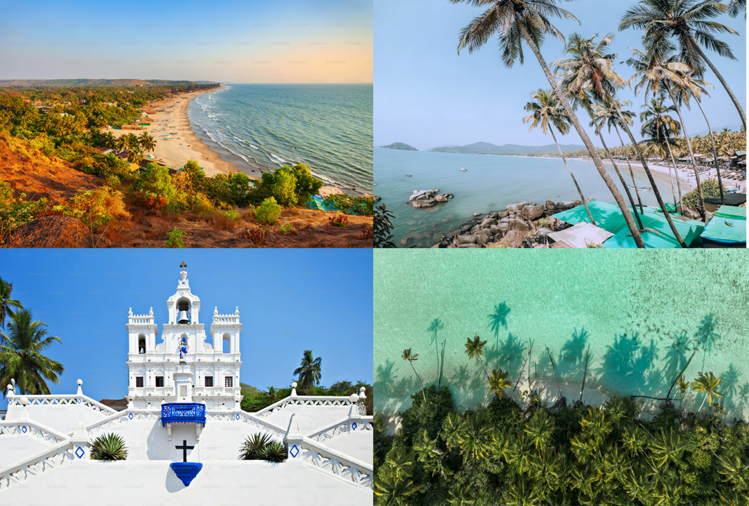
Goa Photos
