


Patents Filed
- White Light Emitting Zinc based OLED
Inventors: Y. N. Mohapatra, S. P. Singh, S. S. Manoharan, and Q. Mohammad Patent No.: 1776/DEL/2004
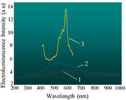
Electroluminescence spectra of unannealed and annealed PPV films (1) CN-PPP films and PPV embedded by Y2O3 (2) PPV structures with the polymer film confined between two metal layers(3)
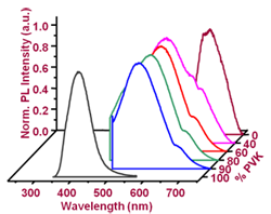 PL spectra with different percentage of PVK
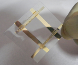
Printed Gold elctrodes and a PVPh dielectric layer on that so as to make a fully inkjet printed device.
Publications
- Sunil Kumar, Upkar K. Verma and Y.N. Mohapatra
Negative contribution to the reverse bias capacitance of organic diodes due to field dependent mobility: determination of barrier height and transport parameters
Journal of Applied Physics,124, 035501 (2018) - Sk Md Obaidulla, Subhash Singh, Y.N. Mohapatra and P. K. Giri
Ambient condition bias stress stability of vanadium (IV) oxide phthalocyanine based p-channel organic field-effect transistors
Journal of Physics D: Applied Physics, 51, 015110 (2018) - Subhash Singh and Y.N. Mohapatra
Bias stress effect in solution-processed organic thin-film transistors: Evidence of field-induced emission from interfacial ions
Organic Electronics, 51, 128-136 (2017) - Upkar K. Verma, Sunil Kumar and Y.N. Mohapatra
Comparison between conventional and inverted solar cells using open circuit voltage decay transients
Journal of Applied Physics, 122, 8, 085503 (2017) - Sunil Kumar, Durgesh C. Tripathi and Y.N. Mohapatra
Organic high-low homojunction diode: Distinct mechanisms underlying forward and reverse bias operation
Organic Electronics, 50, 331-338 (2017) - Upkar K. Verma, Sunil Kumar and Y.N. Mohapatra
Measurement of contact surface photo-voltage from forward bias C-V characteristics of P3HT:PCBM based BHJ solar cells
Solar Energy Materials and Solar Cells, 172, 25 (2017) - Subhash Singh and Y.N. Mohapatra
Origin of switching drain current transients in TIPS-Pentacene based organic thin-film transistor with polymer dielectric: Role of interfacial ions
Applied Physics Letters, 110, 11,233301(2017) - Upkar K. Verma, Durgesh C. Tripathi and Y.N. Mohapatra
Direct determination of defect density of states in organic bulk heterojunction solar cells
Applied Physics Letters,116, 11,113301 (2016) - Subhash Singh and Y.N. Mohapatra
Persistent photocurrent (PPC) in solution-processed organic thin film transistors: Mechanisms of gate voltage control
Journal of Applied Physics, 120, 045501, (2016) - Subhash Singh and Y.N. Mohapatra
Trap Kinetics in Solution-Processed Organic Thin-Film Transistors
IEEE Electron Device Letters, 37, 1, 35-38 (2016) - B. B. Patil, S. S. Mishra and Y.N. Mohapatra
Patent Trends in Printed Electronics and Printed Tags
International Journal of Computer Science and Electronics Engineering, 4, 1, 21-24 (2015) - V. Pandian, Y.N. Mohapatra and V. Kumar
A Review of Photoelectric Properties of EL2 in Semi-Insulating Gallium Arsenide
IETE Journal of Research, 38, 2-3, 70-74 (2015) - Subhash Singh and Y.N. Mohapatra
Dielectric optimization for inkjet-printed TIPS-pentacene organic thin-film transistors
Emerging Electronics (ICEE), IEEE 2nd International Conference (2015) - Mihir Sarkar and Y.N. Mohapatra
Electron beam lithography in thick negative tone chemically amplified resist: Controlling sidewall profile in deep trenches and channels
Microelectronic Engineering,(2014) - Durgesh C. Tripathi and Y.N. Mohapatra
Charge transport across organic heterostructure: Role of interfacial density of states
Journal of Applied Physics, 116, 064509 (2014) - K. Sudheendra Rao, Durgesh C. Tripathi and Y.N. Mohapatra
Carrier capture kinetics at electrical defects in poly [2-methoxy-5-(2′-ethyl-hexyloxy)-1, 4-phenylenevinylene](MEH-PPV) studied using charge transient spectroscopy
Journal of Applied Physics, 116, 054511 (2014) - K. Sudheendra Rao and Y.N. Mohapatra
Open circuit voltage decay transients and recombination in bulk-heterojunction solar cells
Appl. Phys. Lett. 104,203303 (2014) - Mihir Sarkar and Y.N. Mohapatra
Self-aligned electron beam lithography of metallic layer sandwiched in a polymer multilayer: Facilitation of vertical organic transistor fabrication
Microelectronic Engineering,115,16-20 (2014) - Durgesh C. Tripathi, Dhirendra K. Sinha, and Y.N. Mohapatra
Diffusivity and mobility of non-equilibrium carriers in organic semiconductors: Existence of critical field determining temperature dependence
Journal of Applied Physics, 114,154508 (2013) - K S Rao and Y.N. Mohapatra
Disentangling degradation and auto-recovery of luminescence in Alq3 based organic light emitting diodes
Journal of Luminescence Vol. 145,793–796 (2013) - Durgesh C. Tripathi and Y.N. Mohapatra
Diffusive capacitance in space charge limited organic diodes: Analysis of peak in capacitance-voltage characteristics
Appl. Phys. Lett. 102, 253303 (2013) - Mihir Sarkar, Neeraj Shukla and Y.N. Mohapatra
Transmission and charge state distribution of carbon ions emerging from nitrogen gas target in a tandem accelerator: Impact of stripper gas pressure
Physical Review Special Topics-Accelerators and Beams, 15(10),100101 (2012) - Durgesh C. Tripathi and Y.N. Mohapatra
Ideal organic homojunction diode obtained using controlled alignment of localized density of states across doped/undoped interface
Organic Electronics: physics, materials, applications 13 (9) , pp. 1680-1685 (2012) - Dhirendra K. Sinha and Y.N. Mohapatra
Charge trapping and electroluminescence at quantum dots embedded in a polymer matrix
Organic Electronics: physics, materials, applications 13 (8) , pp. 1456-1462 (2012) - Ashish Gupta, Soumen Mandal, Monika Katiyar, and Y.N. Mohapatra
Film processing characteristics of nano gold suitable for conductive application on flexible substrates
Thin Solid Films 520 (17) , pp. 5664-5670 (2012) - Mihir Sarkar, Neeraj Shukla, Nobin Banerji, and Y.N. Mohapatra
Proton beam writing on PMMA and SU-8 films as a tool for development of micro-structures for Organic Electronics
Appl. Surf. Sc. 258 (9) , pp. 4195-4198 (2012) - Awnish K. Tripathi, and Y.N. Mohapatra
Correlation of photocurrent and electroabsorption spectra and their temperature dependence for conjugated light emitting polymers: The origin of the corresponding density of states
Physical Review B 84, 205213 (2011) - Awnish K. Tripathi, Durgesh C. Tripathi,and Y.N. Mohapatra
Simultaneous and direct measurement of carrier diffusion constant and mobility in organic semiconductors and deviation from standard Einstein relation
Physical Review B 84, 041201 (RAPID COMMUNICATIONS) (2011) - Ashish Gupta,Saumen Mandal,Monica Katiyar,and Y.N. Mohapatra
Low Temperature Solution Process forFabrication of Electrodes on FlexibleSubstrate Using Gold Nanoparticles
International Journal of Nanoscience Vol. 10, No. 4 (2011) - Durgesh C. Tripathi, Awnish K. Tripathi, and Y.N. Mohapatra
Mobility determination using frequency dependence of imaginary part of impedance (Im Z) for organic and polymeric thin films
Appl. Phys. Lett. 98, 033304 (2011) - S. K. Sahoo, D. Misra, M. Sahoo, C. A. MacDonald, H. Bakhru, D. C. Agrawal, Y. N. Mohapatra, S. B. Majumder, and R. S. Katiyar
Improved dielectric properties and their temperature insensitivity in multilayered Ba0.8Sr0.2TiO3/ZrO2 thin films
Journal of Applied Physics 109, 064108 (2011) - Santosh K. Sahoo, D. Misra, D. C. Agrawal, and Y.N. Mohapatra
ZrO2 Layer Thickness Dependent Electrical and Dielectric Properties of BST/ZrO2/BST Multilayer Thin Films
Mater. Res. Soc. Symp. Proc. Vol. 1368, 2011 Materials Research Society - S. K. Sahoo, D. Misra, D. C. Agrawal, Y. N. Mohapatra, S. B. Majumder, and R. S. Katiyar
Leakage mechanism of Ba0.8Sr0.2TiO3 /ZrO2 multilayer thin films
Journal of Applied Physics 108, 074112 (2010) - Awnish Kumar Tripathi, Ashish Gupta, Y.N. Mohapatra *
Mobility with negative coefficient in Poole-Frenkel field dependence in conjugated polymers: Role of injected hot electrons
Organic Electronics, Volume 11, Issue 11, November 2010, Pages 1753-1758 - Devendra P. Singh, Y.N. Mohapatra, D.C. Agrawal
Comparative Analysis of unity gain frequency of top and bottom-contact Organic thin film transistors
Materials Science and Engineering: B, Volume 157, Issues 1-3, 15 February 2009, Pages 58-65 - Devendra P. Singh, Y.N. Mohapatra, D.C. Agrawal
Dielectric and leakage current properties of sol-gel derived calcium copper titanate (CCTO) thin films and CCTO/ZrO2 multilayers
Materials Science and Engineering: B, Volume 157, Issues 1-3, 15 February 2009, Pages 58-65 - Dheeraj K. Mohata, Durgesh C. Tripathi and Y. N. Mohapatra
Comparison of Simulation & Experimental Capacitance Based Characterizaton of Organic Semiconductor Diode Structures
Materials Research Society, December, 2008 - Dhirendra K. Sinha Awnish K. Tripathi and Y. N. Mohapatra
Temperature dependence of electroluminescence to isolate the role of CdSe/ZnS Quantum Dots in PFO based polymer light emitting diodes
Materials Research Society, December, 2008 - Vibha Tripathi, M. N. Islam, Y. N. Mohapatra and P. Roca i Cabarrocas
Raman spectroscopy of nano-structured silicon to study the embedded crystallites
Eur. Phys. J. Appl. Phys. 39, 203-209 (2007) - Anand K. Biswas, Ashish, A. K. Tripathi, Y. N. Mohapatra and A. Ajayaghosh
Synthesis, Photophysical and Electroluminescent Properties of Arylenevinylenes-co pryrrolenevinylenes Derived from Divinylaryl Bridged Bispyrroles
Macromolecules, 40, 2657-2665 (2007) - Vibha Tripathi, Y. N. Mohapatra and P. Roca i Cabarrocas
Electrical Manifestation of nanocrystallites embedded in nanostructured hydrogenated Silicon
Journal of Applied Physics 2007 - A.K. Tripathi, R. Verma, A.K. Biswas, Ashish, Y. N. Mohapatra
Electroluminescence transient of polymer light emitting diodes: field dependence of overshoot and time delay
Proc. Of International Workshop on Physics of Semiconductor Devices, 2007, pp 698-601 - A. Dixit, D. C. Agrawal, Y. N. Mohapatra, S. B. Majumder, R.S. Katiyar
Studies on the dielectric and relaxor behavior of sol-gel derived barium strontium zirconate titanate thin films
Materials Letters, Volume 61, Issue 17, July 2007, Pages 3685-3688 - Vibha Tripathi, Y.N. Mohapatra *, P. Roca i Cabarrocas
Trapping phenomena in intrinsic hydrogenated amorphous silicon like materials studied using current transient spectroscopies
Journal of Non-Crystalline Solids vol. 350, 19-20 (2006) 1130-1133 - Samarendra P. Singh, Y.N. Mohapatra , M. Qureshi, S. Sundar Manoharan
Time domain spectroscopic study of PL decay in zinc benzothiazole suitable for white light emitting OLEDs
Synthetic Metals, Volume 155, Issue 2, 15 November 2005, Pages 376-379 - G.S.Samal, A.K.Biswas, Y.N.Mohapatra Electroabsorption spectroscopic study of an electron transport material-CN-PPV Synthetic Metals 155 (2005) 303-305
- G.S.Samal, A.K.Biswas, A.K.Tripathi, Swapnil Singh,Y.N.Mohapatra Photoluminescence quantum efficiency (PLQ) and PL decay dynamics study on polymeric light emitting materials Synthetic Metals 155 (2005) 344-348
- A. K. Biswas, Awnish Tripathi, Swapnil Singh, Y. N. Mohapatra Effect of condensed phase environment on luminescent properties of MEH-PPV thin films Synthetic Metals 155 (2005) 340-343
- Y.N.Mohapatra, V. Varshney, V. Rao, S. P. Singh, G. S. Samal Electrical transient based defect spectroscopy in polymeric and organic semiconductors Mater. Res. Soc. Symp. Proc. Vol. 864, 2005 Materials Research Society E5.1.1
- Vibha Tripathi, Y N Mohapatra, P. Roca i Cabarrocas PECVD grown polymorphous hydrogenated silicon (pm-Si:H) studied using current transient spectroscopies in PIN Diodes Mater. Res. Soc. Symp. Proc. Vol. 862, 2005 Materials Research Society A18.2
- Samarendra P Singh, Y. N. Mohapatra, M. Qureshi, S. Sundar Manoharan White OLED based on spectral broadening in electroluminescence due to formation of interfacial exciplexes Applied Physics Letter 86, 113505 (2005)
- D. Ghosh, G. S. Samal, A. K. Biswas Y. N. Mohapatra Laser Induced degradation Studied of PP and CN-PPV Thin Films using Photoluminescence Thin Solid Films 477 (2005) 162-168
- M. Qureshi, S. Sundar Manoharan , Samarendra P Singh, Y. N. Mohapatra Photogenerated time of flight mobility measurements in novel electron transport material: 2,5-dibenzothiazollyl thiophene Phy. Stat. sol. (a) 201, R60-R63 (2004)
- M. Qureshi, S. Sundar Manoharan , Samarendra P Singh, Y. N. Mohapatra Electroluminescent properties of dimeric bis(2-(2i-hydroxy1phenyl) benzthiazolate) zinc (II) complex Solid State communications 133 (2005) 305-309
- S. K. Sahoo, D. C. Agrawal, Y. N. Mohapatra, S. B. Majumder Ram S. Katiyar Changes in the Leakage currents in BST/ZrO2 multilayers due to modulations in oxygen concentration Appl. Phys. Lett., Vol ,85, No. 21 (2004)
- Sandesh Gupta, D.C.Agarwal Y.N.Mohapatra Photoluminescence of phosphors prepared by low temperature hydrothermal route Journal of the Electrochemical Society, Vol. 151 (11), pp H239-H242, 2004
- V. Ramesh, Y. N. Mohapatra, D. C. Agarwal Depolarization Characteristics of Sol-Gel Pb1.05 (Zr0.53Ti0.47)O3 Thin Film Ferroelectrics: 306:71-77 (2004)
- S. K. Sahoo, D. C. Agrawal, S. B. Majumder, R. S. Katiyar, Y. N. Mohapatra Low Temperature Dielectric Properties of BST/ZrO2 Multilayer Films Proceedings of Materials Research Society, 784, C3.7.1 (2004)
- V. Tripathi , Y. N. Mohapatra P. Roca i Cabarrocas Switch-On Transients And Static Characteristics Of Polymorphous And Amorphous Silicon Thin-Film Transistor Mat. Res. Soc. Symp. Proc. Vol. 762, A18.7.1 (2003)
- V. Tripathi, M. N. Islam, Y. N. Mohapatra, V. Suendo, P. Roca i Cabarrocas Size Distribution Of Embedded Nano-Crystallites In Polymorphous Silicon Studied By Raman Spectroscopy And Photoluminescence Mat. Res. Soc. Symp. Proc. Vol. 762, A19.7.1 (2003)
- Girija Sankar Samal, A. K. Biswas Y. N. Mohapatra Spectroscopic Photovoltage Characterization of PPV thin film suitable for PLED applications Mat. Res. Soc. Symp. Proc. Vol. 771, L7.4.1 (2003)
- Sanjay Rangan, Mark Horn, S. Ashok Y. N. Mohapatra Influence of hydrogen plasma treatment on boron implanted junctions in silicon J. Vac. Sci. Technol. B 21, p781 (2003)
- S.B. Majumder , D.C. Agrawal , Y.N. Mohapatra, R.S. Katiyar Effect of cerium doping on the micro-structure and electrical properties of sol-gel derived Pb1.05(Zr0.53_dCedTi0.47)O3 (d5/10 at.%) thin films Materials Science and Engineering B98, 1 (2003)
- Samarendra P Singh, Vineet Rao, Y.N. Mohapatra, Sanjay Rangan, S. Ashok Electrical signature of ion-implantation induced defects in n-Si in the defect cluster regime studied using DLTS and isothermal transient spectroscopies Defect and Impurity Engineered Semiconductors and Devices Materials Research Society Vol. 719, p F11.1 (2002)
- Y.N. Mohapatra Semiconductor Defect Characterization Deep Level Transient Spectroscopy Techniques, One Day Tutorial conducted at MRS 2002 (San Francisco) under the Symposium on Defect and Impurity Engineered Semiconductors and Devices Notes distributed by Materials Research Society (Waarandale, PA) 2002
- V. Tripathi, M. N. Islam, S. Gupta and Y. N. Mohapatra Raman Spectroscopy of Polymorphous silicon to study embedded nanocrystallites Proc. Of Sixth Intl. Conf. Optoelectronics, Fibre Optics, and Photonics, OMD-33, Mumbai (2002)
- Samarendra P. Singh, Y.N. Mohapatra, Sanjay Rangan and S. Ashok Carrier Dynaics at deeap traps in ion implanted silicon: Possible Signature of Defect Clusters Physics of Semiconductor Devices ,ed. V. Kumar and P.K. Basu, Allied , p 1025 (2002)
- S.B. Majumder, D.C. Agarwal, Y.N. Mohapatra and R.S. Katiyar
Microstructure Evolution and Electrical Characteristics of Ce doped PZT thin films Proc. Annual Meeting of American Ceramic Society, St. Luis (2002) - A. Singh, Y.N. Mohapatra and Satyendra Kumar
Electromagnetic induction and damping: Qualitative experiments using PC interface Am. J. Phys. 70 (2002) 424 - P.K. Giri and Y.N. Mohapatra Evidence of Metastability with athermal ionization from defect clusters in ion-damamged silicon Phys. Rev. B62, pp16561-16565 ( 2000)
- P.K. Giri and Y.N. Mohapatra Capacitance Transient Spectroscopy Models of coupled trapping kinetics among multiple defect states : application to multiple defects due to heavy ion damage in silicon Phys. Rev. B62, pp2496-2504 ( 2000)
- P.K. Giri and Y.N. Mohapatra Thermal Stability of Defect Complexes due to high dose MeV implantation in silicon Mat. Sc. Engg. B 71, p.327, 2000
- S.B. Majumder, B. Roy, D.C. Agrawal and Y.N. Mohapatra Fatigue and dielectric properties of undoped and Ce doped PZT thin films Integrated Ferroelectrics, 225, A63-A74 , (2000)
- S.B. Majumder, B. Roy, D.C. Agrawal and Y.N. Mohapatra Phase Transformations in So-Gel Prepared PZT and PLT Thin Films upon Isothermal Treatmentsat Different Temperatures Ferroelectrics, 225, pp. 271-278 , 1999
- P.K.Giri and Y.N.Mohapatra Electrical Characterization of MeV Heavy Ion Induced Damage in silicon : Evidence of defect migration and clustering J. Appl. Phys. 84, pp 1901-1911 (1998)
- P.K.Giri, Sankar Dhar, V.N.Kulkarni, and Y.N.Mohapatra Charge redistribution among defects in heavily damaged silicon Phys. Rev. B 57, pp14603-14607 (1998)
- P.K Giri and Y.N. Mohapatra Compensating defects in deep buried layers produced by MeV heavy ions in n- silicon Appl. Phys. Lett. 71, pp 1682-1684 (1997)
- P.K. Giri, S.Dhar, V.N. Kulkarni and Y.N. Mohapatra Electrically active defects in as-implanted deep buried layers in p-type silicon J. Appl. Phys. 81, pp 260-263 (1997)
- S.B. Majumder, Y.N. Mohapatra and D.C. Agarwal Fatigue Resistance in Lead Ziconate Titanate thin ferroelectric films : Effect of Cerium doping and frequency dependence Appl. Phys. Lett. 70, pp 138-140 (1997)
- S.B. Majumder, Y.N. Mohapatra and D.C. Agarwal Optical and Microstructural Characterization of sol-gel derived Ce-doped PZT thin films Journal of Materials Science 32, pp 2141-2150 (1997)
- P.K. Giri, S. Dhar, V.N. Kulkarni and Y.N. Mohapatra Characterization of deep level defects in Si irradiated with MeV Ar ions using constant capacitance time analyzed transient spectroscopy Bulletin of Mater. Science 20, pp417-421, (1997)
- S.B. Majumder, Y.N. Mohapatra and D.C. Agarwal Optical and Microstructural Characterization of sol-gel derived Cerium doped PZT thin films J. Mater. Science, 32, pp2141-2150 (1997)
- S.Dhar, T.Som, Y.N. Mohapatra and V.N. Kulkarni Ar ion induced copper germanide phase formation at room temperature Bulletin of Mat. Sc., 20, p423-427 (1997)
- P.K. Giri, S.Dhar, V.N. Kulkarni and Y.N. Mohapatra Electrically active defects due to end-of-ion range damage in silicon irradiated with MeV Ar+ ion Nucl. Inst. Meth. B, 111, pp 285-289 (1996)
- S.Dhar, Y.N.Mohapatra and V.N. Kulkarni Compound formation under local thermal spikes during ion-bem mixing : Model and its experimental verification Phys. Rev. B 54, pp 5769-5476 (1996)
- Sandeep Agarwal, Y.N.Mohapatra, Vijay A.Singh and R.Sharan
Time analyzed transient spectrscopy and multiple DX related emission centres in silicon doped AlxGa1-xAs J. Appl. Phys. 77, pp 5725-5729 (1995) - Sandeep Agarwal, Y.N.Mohapatra, Vijay A.Singh Temperature - time duality and deep level spectroscopies J. Appl. Phys. 77, pp 3155-3161 (1995)
- P.K.Giri and Y.N.Mohapatra Nonexponentiality in photoinduced current transients in undoped semi - insulating gallium arsenide J. Appl. Phys. 77, pp 262-268 (1995)
- S.Dhar, T.Som, Y.N.Mohapatra and V.N. Kulkarni
Room temperature synthesis of copper germanide phase by ion beam mixing Appl. Phys. Lett. 67, pp1700-1703 (1995) - Sandeep Agarwal and Y.N.Mohapatra The Kinetics of capture and emission of discrete DX related centres in silicon doped AlGaAs using time analyzed transient spectroscopy Materials Science Forum, vol. 378 , pp 941-946 (1995)
- S.B.Majumdar, D.C.Agarwal, Y.N.Mohapatra and V.N.Kulkarni Perovskite Phase Formation in sol-gel derived lead ziconate titanate thin films Integrated Ferroelectrics 9, pp 271-284 (1995)
- S.B.Majumdar, V.N. Kulkarni, Y.N.Mohapatra and D.C. Agarwal Interfacial Mechanisms controlling phase formation in sol-gel derived lead zirconate titanate thin films Bull. Mat. Sci. 17, pp. 1005 - 1014 (1995)
- D.C.Agarwal,S.B.Majumdar,Y.N.Mohapatra, R. Sataiah,H. D. Bist, R. S. Katiyar
Micro-Raman studies of sol-gel derived lead zirconate titanate thin films Raman Spectroscopy 24, pp 459-462 (1993) - V.Pandian, Y.N.Mohapatra and V. Kumar
Photoelectric properties of EL2 in semi-insulating GaAs IETE 38, 70-76 (1992) - V.Pandian, Y.N.Mohapatra and V. Kumar
Gold and silver related deep level defects in GaAs J. Appl. Phys. 30, pp 2815-2820 (1991) - Y.N.Mohapatra and V. Kumar
Trapping characteristics of DX centres in MBE grown GaAlAs J. Appl. Phys. 68, pp 3431-3434 (1990) - Y.N.Mohapatra and V. Kumar
Characterization of defects in gallium arsenide Bull. Mater. Sci 13, pp 83-88 (1990) - Y.N.Mohapatra and V. Kumar
Temperature dependence of photocurrent in undoped semi-insulating gallium arsenide Phys. stat. solidi (a) 114, pp 659-663 (1989) - Y.N.Mohapatra and V. Kumar
Determination of activation energy for thermal regeneration of EL2 metastable state by thermally stimulated photocurrent measurements J. Appl. Phys. 64, pp 956-958 (1988) - S.Subramaniam, B.M.Arora, Y.N.Mohapatra and V. Kumar
Trapping characteristics of dual states of the DX centre in MBE grown si doped GaAlAs in 'Defects in Semiconductors eds. H.J. von Berdeleben, Materials Science Forum, vol. 10 - 12 , pp 405-411 (1986) - Y.N.Mohapatra N. Balasubramaniam and V. Kumar
Characterization of deep levels in semi-insulating gallium arsenide Bull. Mater. Sci. 7, pp 57-61 (1985)
Conference Proceedings (Selected)
- Sunil Kumar, Upkar K. Verma, Y. N. Mohapatra Determination of defect density of states in organic diodes using capacitance-voltage measurements International Conference on Advanced Nanomaterials and Nanotechnology, ICANN-2017
- Santosh K. Sahoo, H. Bakhru, Sumit Kumar, D. Misra, Colin A. Wolden, Y. N. Mohapatra and D. C. Agrawal, Field Dependent Carrier Transport Mechanisms in Metal-Insulator–Metal Devices with Ba0.8Sr0.2TiO3/ ZrO2 Heterostructured Thin Films as the Dielectric, MRS Proceedings / Volume 1547 / 2013
- Anshul Sharma, Ashish Gupta, Y. N. Mohapatra Synthesis of silver nanoparticles for printable electronics International Conference on Nano Science and Technology (ICONSAT) Mumbai, February 17-20, 2010
- Ashish Gupta, Saumen Mandal, Monika Katiyar, Y. N. Mohapatra Low temperature solution process for fabrication of electrodes on flexible substrate using gold nanoparticles International Conference on Nano Science and Technology (ICONSAT) Mumbai, February 17-20, 2010 (Best Poster Award)
- Lalat I. Giri, Durgesh C. Tripathi, and Y. N. Mohapatra Field and Thickness Dependence of Mobility of Organic Semiconductors determined using Photocurrent Transients Proceedings of the 15th International Workshop on the Physics of Semiconductor Devices, New Delhi, Dec., 2009.
- Ashish Gupta, Anand K Biswas, Awnish K Tripathi and Yashowanta N Mohapatra Side Chain Influence On The Optical Properties of Conjugated Arylenevinylenes-Co-Pyrrolenevinylenes(AVPV) Presented in the XV International Workshop on the Physics of Semiconductor Devices, New Delhi, 15th -19th Dec. 2009
- Ashish Gupta, Saumen Mandal, Priyanka, Monica Katiyar, Y. N. Mohapatra Nano gold ink for printing micro structure on flexible substrate DAE-BRNS 2nd Internation Symposium on Materials Chemistry, Dec. 2-6, 2008.
- D.C. Tripathi, D.K.Sinha, C.K.Suman and Y. N. Mohapatra Electrical Characterization of Solution Processed MEHPPV/CNPPV Hetrostructure 9th Asian Symposium on Information Display, New Delhi, 2006, pp 219
- Samarendra P. Singh. Mohammad Qureshi, S. S Manoharan and Y. N. Mohapatra DLTS studies on Organic/Inorganic heterostructure devices Proceedings of the 12th International Workshop on Physics of Semiconductor Devices 2003, Ed. K. N. Bhatt & A. DasGupta. Vol. 2, pp-1219-1221 Narosa Publishing House New Delhi
- G.S.Samal, Subhadip Mitra, Rahul Dubey, and Y. N. Mohapatra Internal Electric Field and Contact Potential in Polymer Light Emitting diode structure studied by Electroabsorption Spectroscopy Proceedings of the 12th International Workshop on Physics of Semiconductor Devices 2003, IIT Chennai, India.
- G. S. Samal, A. K. Biswas, Y. N. Mohapatra Temperature Dependence of Photoluminescence Spectra of PPV and CN-PPV Thin Films Presentation on 2nd International conference on materials for advanced technologies & IUMRS-International conference in Asia 2003 December 7-12, Singapore
- G.S.Samal, A.K.Biswas and Y. N. Mohapatra Spectroscopic Photovoltage Characterization of PPV Thin Films Suitable for PLED Applications MRS Proceeding Symposium Spring 2003
- Y. N. Mohapatra and P. K. Giri Sensitivity of electrically active defect spectra to processing conditions in MeV heavy ion implanted silicon Proceedings of MRS Spring Meeting 99 : Front End Processing in silicon ed. H-J Gossmann (1999)
- Y. N. Mohapatra and P. K. Giri Charge redistribution and defect relaxation in heavily damaged silicon studied using time analyzed transient spectroscopy Defect and Impurity Engineered Semiconductors and Devices II : ed. S.Ashok, JCChevallier, K. Sumino, B.L. Sopori and W. Gotz, MRS 98 Spring Meeting (San Francisco) Symposium Proceedings vol 510, pp349-354 (1998)
- Y. N. Mohapatra and P. K. Giri Evidence of defect migration and clustering in MeV heavy ion damaged silicon Defect and Impurity Engineered Semiconductors and Devices II : ed. S.Ashok, JCChevallier, K. Sumino, B.L. Sopori and W. Gotz, MRS 98 Spring Meeting (San Francisco) Symposium Proceedings vol 510, pp403-409 (1998).
- T.Som, Sankar Dhar, Y.N. Mohapatra and V.N. Kulkarni
Study of Plsma Ion Implanted Hydrogen in Semi-insulating GaAs Physics of Semiconductor Devices ,ed. Vikram Kumar, S.K. Agarwal, vol II, pp369-372, (Narosa, New Delhi) 1997 - P. K. Giri, S. Dhar, V.N. Kulkarni and Y. N. Mohapatra
Trapping characteristics of MeV ion implanted buried layers in silicon DAE Solid State Symposium, Mumbai, India , Dec 27-31, 1996 - P. K. Giri, S. Dhar, V.N. Kulkarni and Y. N. Mohapatra
Electrically active defects due to end-of-ion range damage in silicon irradiated with MeV Ar+ ion National Conference on Recent Advances in in Semiconductors, New Delhi, India June 20-22 1995 Semiconductor Materials and Devices, eds. O.P. Agnihotri and V. K. Jain (Narosa, New Delhi) 1997, pp 140-146 - P. K. Giri and Y.N. Mohapatra
Time Analyzed Transient Spectroscopy Analysis of Photo-induced Current Transients in Undoped Semi-insulating Gallium Arsenide National Conference on Recent Advances in in Semiconductors, New Delhi, India June 20-22 1995
Semiconductor Materials and Devices, eds. O. P. Agnihotri and V. K. Jain (Narosa, New Delhi) 1997, pp 156-160 - P. K. Giri, S. Dhar, V. N. Kulkarni and Y. N. Mohapatra
Characterization of deep level defects in Si irradiated with MeV Ar+ ions using constant capacitance time analyzed transient spectroscopy
International Conference on Defects in Condensed Media, Kalpakkam, India, September 20-22, 1995 - S. Dhar, T. Som, Y.N. Mohapatra and V. N. Kulkarni
Ar ion induced copper germanide phase formation at room temprature International Conference on Defects in Condensed Media, Kalpakkam, India, September 20-22, 1995 - S.B. Majumdar, D.C. Agarwal, Y. N. Mohapatra and V. N. Kulkarni
Mechanisms controlling phase formation in PZT thin films by sol-gel technique Proc. Ninth IEEE International Symposium on Applications of Ferroelectrics (ISAF-94), eds. R.K. Pandey, M.Liu and A.Safari, August 1994, Pennsylvania USA - S.B. Majumdar, D.C. Agarwal, Y. N. Mohapatra and V. N. Kulkarni
Preparation and Characterization of PZT thin films by sol-gel technique National Seminar on Ferroelectric Device and Laser Materials, Nagpur University, Nagput (India) 1994 - B. Bhattacharya, S, Dhar, K. Ramakrishnan, V.N. Kulkarni and Y. N. Mohapatra Synthesis of copper germanide films by ion beam mixing Solid State Physics (India), 37C, 458 (1994)
- S. Agarwal, P.K. Giri, R. Sharan and Y. N. Mohapatra Evidence of field dependent emission from DX centres Proc. of 7th International Workshop on Physics of Semiconductor Devices, ed. K.Lal (Narosa, New Delhi) 1993
- M.N. Islam, Y. N. Mohapatra, S. C. Agarwal and S. Kumar Electron transport mechanism in amorphous silicon Schottky barrier devices Proc. 7th International Workshop on Physics of Semiconductor Devices, ed. K.Lal (Narosa New Delhi) 1993, p405
- Y. N. Mohapatra and V. Kumar
Kinetics of capture and emission of multiple states of DX centres Proc. of 3rd International Workshop on Physics of Semiconductor Devices, ed. Radhakrishnan (Madras) 1987
Tutorials Conducted in International Conferences
- Tutorial (Full day) 0n "Semiconductor Heterostructures", San Francisco, MRS 2008
- Tutorial (Half-day) on "Organic Semiconductors" at TIFR, Mumbai, organized by International Workshop on Physics of Semiconductor Devices, IWPSD 2007.
- Tutorial (Half-day) on "Organic Light Emitting Displays" at India Habitat Centre,New Delhi, organized by ASID 06, October (2006)
- Tutorial (Full day) 0n "Deep Level Transient Spectroscopy (DLTS)", San Francisco, MRS2003
Invited Lectures in Meetings and Conferences (Selected)
- Mobility, Diffusivity and Relaxation in Organic Semiconductors: Measurements that Challenge Models Invited Lecture delivered at Institute of Materials Research, Singapore in Symposium on Organic & Polymer Electronics: IMRE, December 9-10, 2010 Singapore
- Lecture on Transport and Injection of Carriers in organic Semicondcutors in SCDT Orgaqnic Electronics Course Indian Institute of Technology, Kanpur July 05, 2010
- Lecture on Transport and Injection of Carriers in organic Semicondcutors in SCDT Orgaqnic Electronics Course Indian Institute of Technology, Kanpur July 2009
- Embedded Nanostructures in Semiconductors for Photovoltaic Applications IOP and KIIT Presentation 25 January, 2009
- Electrical Characterization of Semiconductors and Deep Level Transient Spectroscopy (DLTS) Characterization SSPL New Delhi 15 January, 2009
Invited Lecture on Embedded Nanoscale Heterostructures for Photoelectronic Applications Polymers for Optoelectronic Applications
Delivered at Jamia-Millia Islamia, National Nanotechnology Seminar, January 30 (2008)Delivered Medal Lecture on Organic Semiconductors as Electronic Materials: Impact of Defects and Disorder induced DOS
MRSI Medal Lecture , Annual General Meeting of Indian Materials Society Trivandrum, February 18(2008)- ICPR Periodical Lecture in "Practical and Theoretical Rationality" This lecture, entitled "Scientific Rationality" was delivered by Professor Y N Mohapatra, Department of Physics, Indian Institute of Technology, Kanpur, on Friday, 14 March, 2008.
- Lecture in SCDT Orgaqnic Electronics Course Indian Institute of Technology, Kanpur July 2008
- Molecular Semiconductors : Strategies to understand & Optimize Materials for Devices Fourth JNC Conference on Chemistry of : Materials September 27, 2008 Alleppy
- Polymeric Semiconductors :Displays & Electronic Applications Photonics India Review Oct 16, 2008 IISc Bangalore
- Embedded Nanostructures in Organic Semiconductors NPL New Delhi 24th December, 2008
- Organic Semiconductors for Displays and Photonic applications Photonics ,BITS Pilani
- Engineers Day Theme Lecture on Convergence of Technologies for Rapid Development
Professor Y. N. Mohapatra delivered the talk on this topic during the celebrations organized by the Kanpur Chapter of the Institution of Engineers at IIT Kanpur on September 15, 2007
- Delivered an Invited Lecture on Nanotechnology : A tour of some recent developments L.N.M. I.I.T, Jaipur, on December 31 (2007)
- Transport in Organic Semiconductors: A Primer on Practice and Problems Short Course on Organic Electronics, SCDT, IIT Kanpur June25-July 20 (2007)
- Transport in Organic Semiconductors: A Primer on Practice and Problems Short Course on Organic Electronics, SCDT, IIT Kanpur June25-July 20 (2007)
- Half Day Tutorial on Organic Semiconductors at TIFR, Mumbai International Workshop on Physics of Semiconductor Devices, (IWPSD) 2007.
- Liquid Crystal Displays: An Introduction Short course on Audio and Video Processing, Coding and Displays held at IIT Kanpur, Nov 26-Dec.06, 2007
Invited Lecture on Evolution of Photo- and electro-luminescence Spectra in Blends of red emitting AVPV Oligomer and PVK
A. K. Biswas, Awnish Tripathi, A. Ajayaghosh and Y. N. MohapatraInvited Oral Presentation in 10th International Conference on Advanced Materials, 9-13 October, IURS-ICAM, Bangalore, 2007
- The Exciting Frontiers of Physics: A tour of some random spots National Workshop on Innovative Physics Experiments, IIT Kanpur, June 11, (2007)


