Research Interests

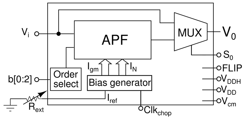
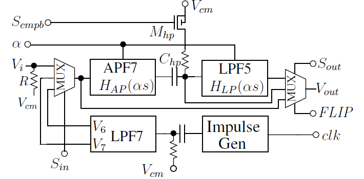
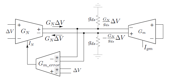
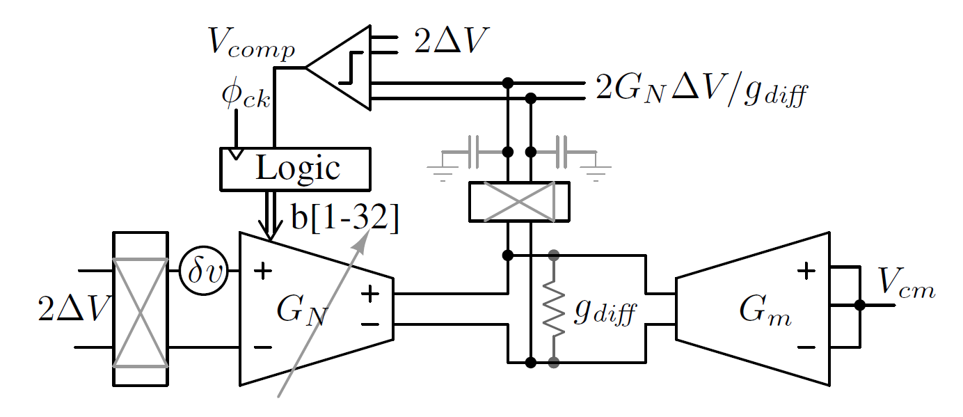
I work in the domain of analog circuit design for integrated circuits, primarilly aimed at signal processing. This involves conceptualization of the problem statement, designing an analog circuit solution, sending out the chip for fabrication (typically called tape-out), designing the PCB for testing the chip, and finally validating the simulation results through measurement results of the chip. My research work till date has concentrated on design of high frequency analog filters for various applications like design of true-time-delay elements for wideband beamformers on integrated circuits, and expansion and compression of wideband analog pulses.

If you are intersted in working with me, do apply for research positions through the IITK portal, and send me your C.V. There are open research positions both for M.S. and Ph.D. candidates. You can learn more about the programs here.


Some previous works are briefly highlighted here:
.
“A 2 GHz bandwidth, 0.25-1.7 ns true-time-delay element using a variable-order all-pass filter architecture in 0.13 μm CMOS"

In this work we designed and demonstrated wide-band true-time-delay lines using integrated circuit Gm-C filters. The proposed architecture achieved state-of-the-art delay-bandwidth product among all the true-time-delay lines hitherto reported at the time of publication.
“Expansion and compression of analog pulses using bandwidth switching of continuous-time filters"

This work was a first demonstration of an integrated circuit implementation of expansion and compression of continuous-time, wideband analog pulses. Pulse expansion and compression factors of 1.8x and 1.7x respectively were demonstrated using electronically controlled bandwidth switching of Gm-C filters.
“Gain enhanced high frequency OTA with on-chip tuned negative conductance load"

This work proposed a transconductor architecture useful for wideband Gm-C filters which can achieve large unity gain frequency without compromising DC gain. An automatically controlled, incremental negative conductance load was designed to cancel the incremental positive conductance of the transconductor across process, voltage and temperature variation.
“Linearity and gain enhanced wideband transconductor using digitally auto-tuned negative conductance load"

This work proposed a voltage biased transconductor with improved linearity (higher signal handling capacity) and high DC gain using a digitally auto-tuned negative conductance load.