 Mohit D. Ganeriwala Mohit D. Ganeriwala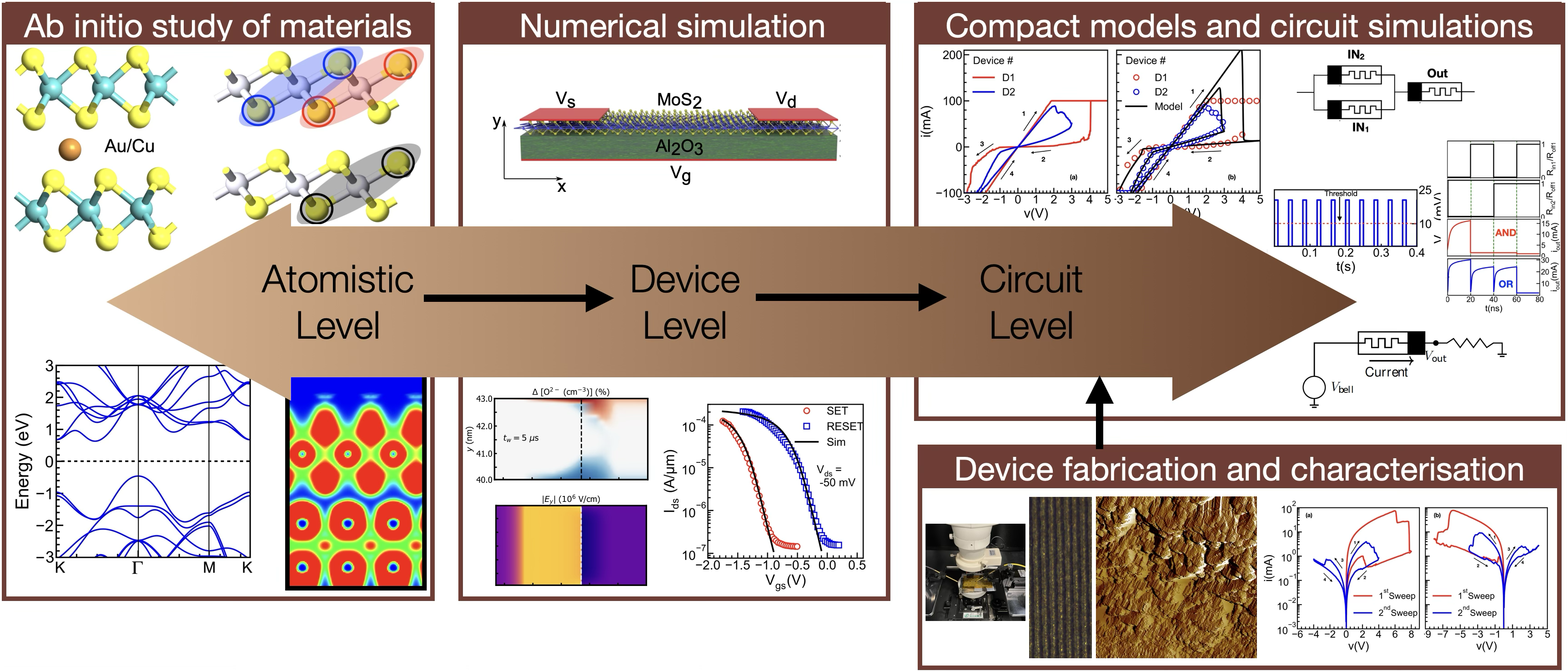
Richard P. Feynman's 1959 lecture, "Plenty of Room at the Bottom," articulates a philosophy that is increasingly pertinent in contemporary societies; where humanity has progressed toward extreme technological miniaturization. We have reached the capability to manipulate nature from its more fundamental components i.e. the atoms, incidentally blurring the boundaries between various fields of study. While conventional electronics continue to downscale aggressively toward sub-nanometer dimensions, emerging two-dimensional (2D) materials, has introduced an electronic “Lego land” offering vast possibilities and already demonstrating significant applications. At NEXT Lab we focuses on the investigation of materials and devices, for next generation computing applications employing a bottom-up approach that starts from the atomic level and scales up to circuits. For which we employs a multi-scale simulations and modeling framework, and apply these techniques to following areas.
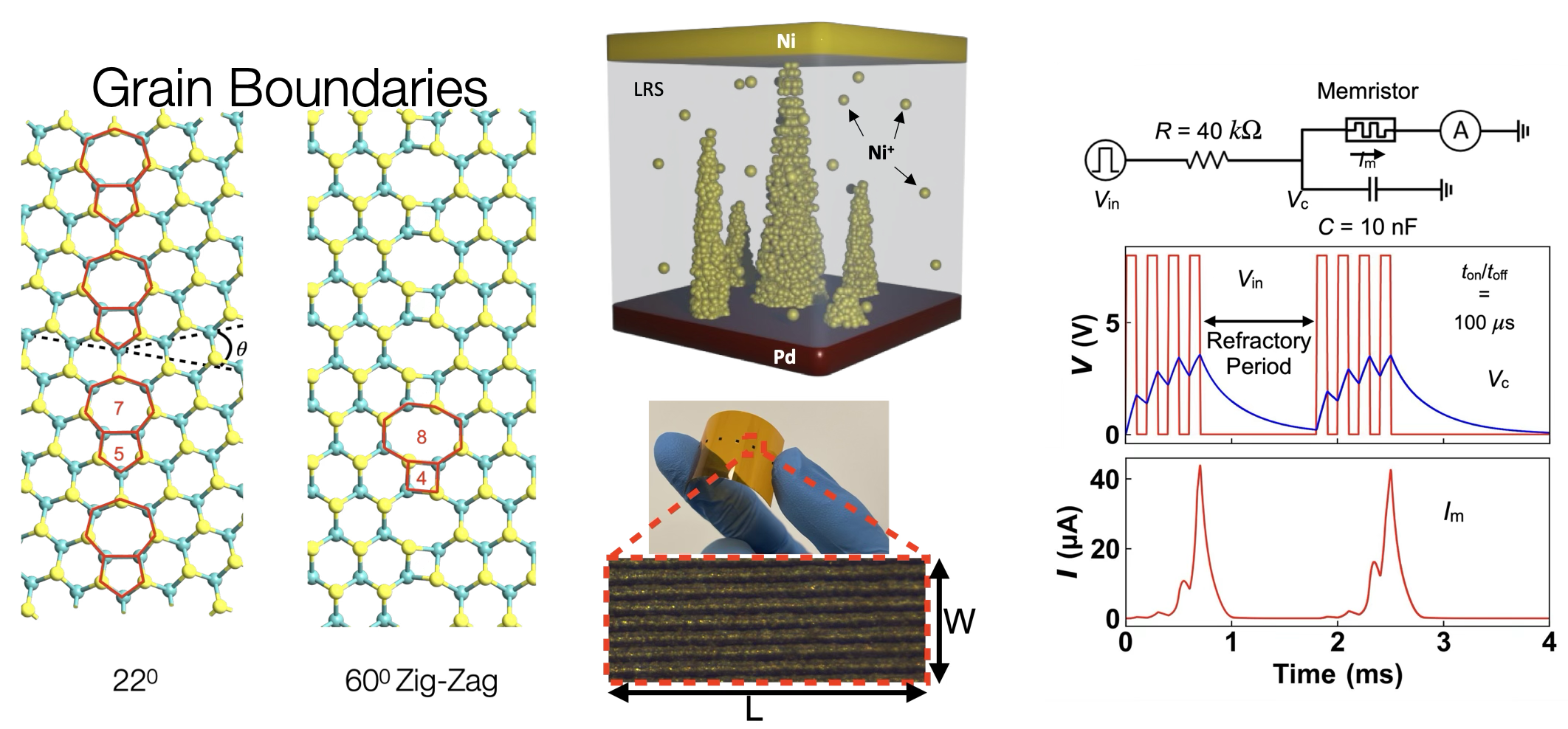
We investigate two-dimensional (2D) materials-based resistive switches for their potential applications as artificial synapses and neurons. Our research focuses on the following key areas:
a) Atomistic Modeling: Exploration of defects and grain boundaries to understand their impact on device behaviour.
b) Device-Level Simulation: Development of numerical tools, in conjuction with commercial CAD software to analyze device characteristics, with particular emphasis on mixed ionic–electronic conduction.
c) Compact Modeling and Circuit Integration: Creation of compact models for various 2D resistive switches and their implementation in circuit-level simulations to emulate neuromorphic functionality.
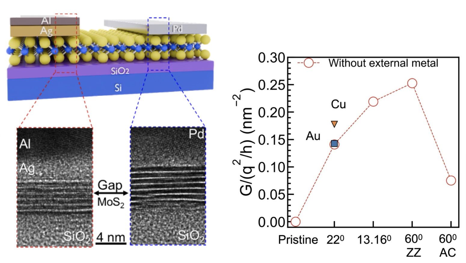
We explore two-dimensional (2D) materials-based Field-Effect Transistors (FETs), including reconfigurable FETs, for next-generation electronic applications. Our research focuses on the following key areas: a) Atomistic Modeling: Investigating electron transport properties at the atomic scale to understand and optimize device performance. b) Device-Level Simulation: Performing detailed simulations of 2D materials-based transistors to analyze and predict their electrical characteristics. c) Compact Modeling and Circuit Design: Developing compact models and conducting circuit-level simulations to enable integration of 2D FETs into advanced electronic systems.
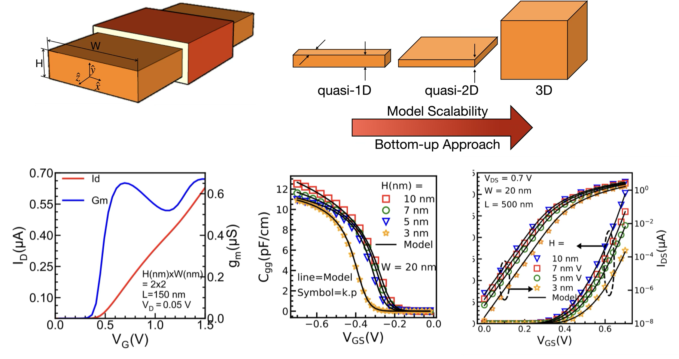
The advanced 3D architecture enables the industry to push Moore's Law into the deep sub-nanometer regime. We focus on investigating the new phenomena that arise as device dimensions approach the quantum limit. We develop compact models to capture these effects analytically without relying on empirical curve fitting. The models ensure continuous scalability from bulk architectures to extremely confined structures. We also analyze non-idealities such as defects and traps in these structures, which affect device noise and reliability.
IIT Kanpur
IIT Gandhinagar
IIT Ropar
University of Granada, Spain
RWTH Aachen, Germany
University of Texas Austin, USA
Universidad Autonoma de Madrid, Spain