
Dr. Avinash Lahgere
Assistant Professor
Department of Electrical Engineering
Indian Institute of Technology Kanpur, India

Ongoing Projects
| S.No | Role | Project Title | Funding Agency | Budget (Rs.) | Duration |
|---|---|---|---|---|---|
| 1 | PI | Reliability Characterization and Modeling of CMOS Devices | IIT Kanpur | 25 Lakhs | 2022-2025 |
| 2 | PI | Evaluation of Radiation Resiliency on Emerging Single Transistor Dynamic Random Access Memory | Science and Engineering Research Board (SERB) | 41 Lakhs | 2023-2026 |
| 3 | PI | Reliability Characterization of CMOS Devices Measurement Lab: IIT Kanpur | IIT Kanpur | 1.05 Crore | 2023–2025 |
| 4 | Co-PI | RF Characterization and Compact Modeling of Wide Band-Gap Gallium Nitride (GaN) Devices for the Next Generation Wireless Communication | Science and Engineering Research Board (SERB) | 68.31 Lakhs | 2024-2027 |
| 5 | Co-PI | Design and Technology Co-optimization of Stacked Nanosheet RF for 6G Applications | Indian National Academy of Engineering (INAE) | 40 Lakhs | 2024-2027 |
| 6 | MPI | Design and Demonstration of Highly Scalable Quantum Computer using Semiconducting Quibts | DST NQM | 3.96 Crore | 2024 - 2027 |
| 7 | PI | Sub-6 GHz RF PA Design using Cadence AWR Suite | Cadence | Undisclosed | 2024-2025(Renew every year) |
| 8 | PI | Cryo-CMOS PDK Enablement for Semiconducting Qubit: Cryogenic Probe Station | IIT Kanpur | 3 Crore | 2025-2026 |
| 9 | Co-PI | Synergistic Development of Semiconductor and Digital Technologies for Automotive Sector | ANRF PAIR | 2.3 Crore | 2025-2026 |
Research Areas

CMOS and Beyond CMOS
To enhance computing performance, a transistor with a small feature size is required to perform better at higher speeds. However, the aggressive scaling of CMOS results in increased short channel effects (SCEs), which restricts the scaling of the CMOS in the sub-10 nm regime. Also, the ever-increasing role stress engineering effect due to scaling raises a major concern regarding the local layout effect (LLE). In this area, we would like to address the scaling and LLE challenges of the CMOS. Broadly, our research efforts are:
1.Developing novel devices and circuits for more-of-Moore and more-than-Moore applications
2.Investigating emerging device architecture incorporating new materials that will enable aggressive operating voltage scaling for energy efficient computing applications

Compact Modelling
A compact model is a mathematical representation of all the physical phenomena encountered in semiconductor devices as shown by technology for Computer-Aided Design. The compact model helps to anticipate circuit functionality, performance, and even yield prior to wafer processing. It allows circuit sensitivity analysis such as temperature, voltage supply, or process variations. With the continuous miniaturization of technology nodes, several new effects are coming into the actions, which need to be modeled. In this regard, the key research objectives are:
1.Develop a compact model for novel CMOS devices and circuits
2.Develop a compact model for statistical effects
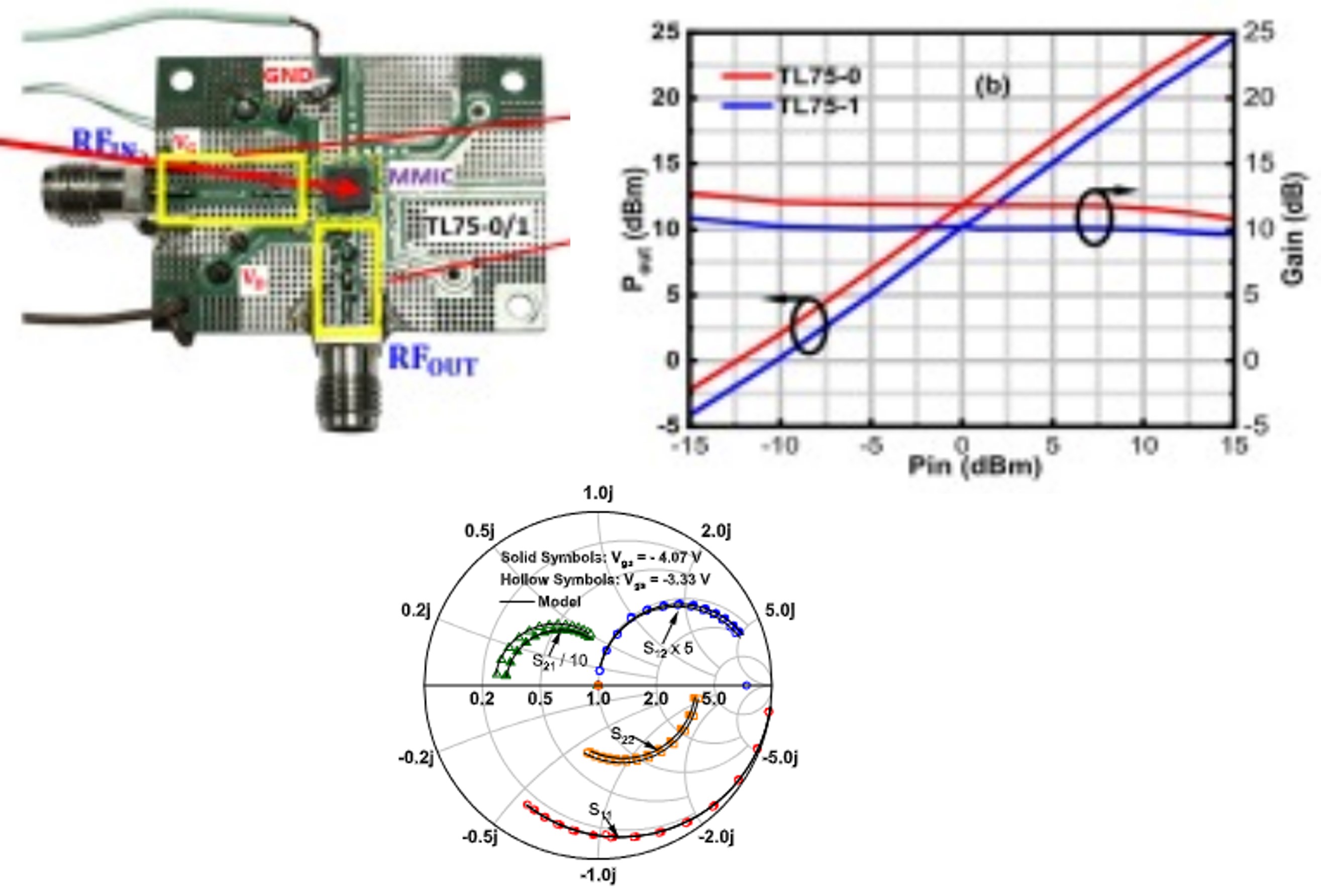
GaN HEMT based RF Circuits
The growing demand for the millimeter-wave (mmW) band (30-300 GHz) is driven by its shorter wavelengths and wider frequency bands, enabling the development of smaller components with enhanced performance. Monolithic microwave integrated circuits (MMICs) based on GaN technology play a critical role in fulfilling the requirements of the mmW range. Our reserach interest focused on:
1.Develop a compact model for D-model and E-mode Gan HEMT devices
2.Examination of GaN-based devices for mmW applications, such as high-power amplifiers, and low noise amplifiers

Electrostatic Discharge (ESD) Protection
Electrostatic discharge (ESD) is a serious threat in the semiconductor industry, capable of causing failures and damage in electronic devices due to rapid electrical charge transfer. Voltages during ESD incidents can exceed device limits, resulting in failures like dielectric breakdown and thermal damage etc. Therefore, our reserach interest focused on:
1.Develop a compact model for ESD protection devices.
2.Investigation novel device architectures for ESD design.
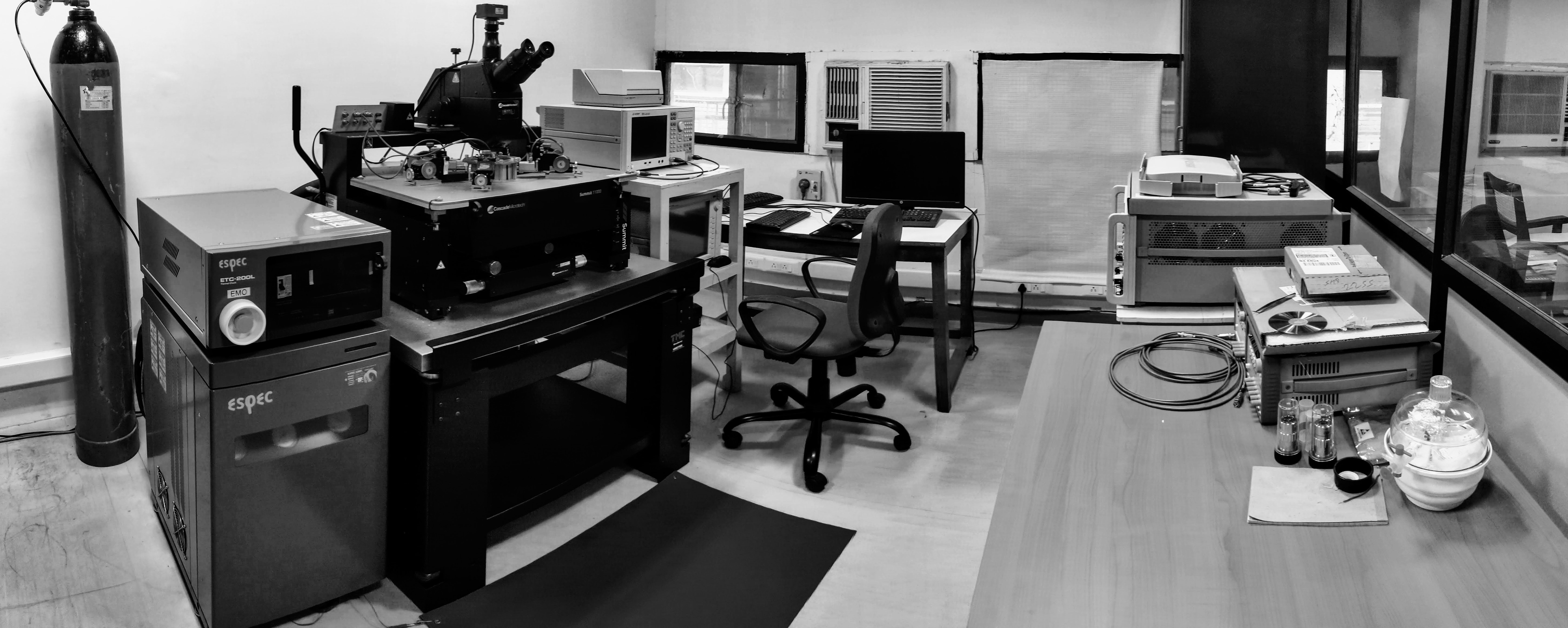
Research Facilities
| S.No. | Equipment Name | Model | Uses |
|---|---|---|---|
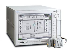
| 1 | Semiconductor device characterization systems(DC & CV) | B1500 | Keysight B1500A Semiconductor Device Analyzer of Precision Current-Voltage Analyzer Series is an all in one analyzer supporting IV, CV, pulse/dynamic IV and more, which is designed for all-round characterization from basic to cutting-edge applications. |
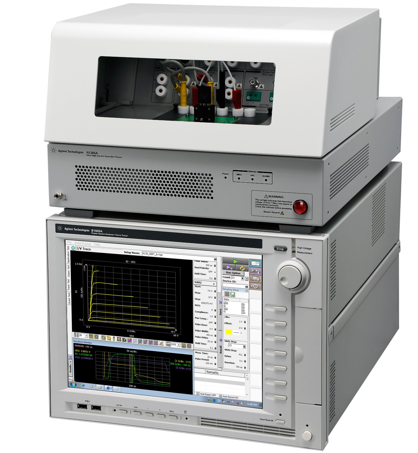
| 2 | Power device characterization systems | B1505 | The Keysight B1505A Power Device Analyzer / Curve Tracer is the only single box solution available with the capability to characterize high power devices from the sub-picoamp level up to 10 kV and 1500 A.These capabilities allow evaluation of novel new device such as IGBT and materials such as GaN and SiC. |
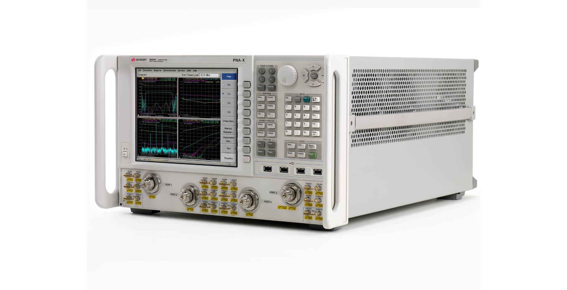
| 3 | RF measurement system | N5244A | The combination of two internal signal sources, a signal combiner, S-parameter and noise receivers, pulse modulators and generators, and a flexible set of switches and RF access points provide a powerful hardware core for a broad range of linear and nonlinear measurements, all with a single set of connections to the device-under-test (DUT). |
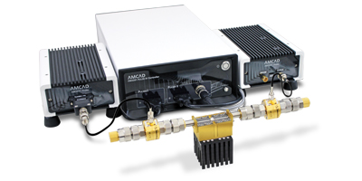
| 4 | Pulsed IV system | Maury Microwave AM3200 | AM3200 is a useful instrument for all the Pulse IV or Load Pull applications. This Pulse IV system is used to bias transistors in quasi-isothermal conditions, it enables accurate compact modeling activities. The system consists of two independently operating power modes: Pulsed or DC (continuous mode). |
| 5 | Wafer level measurement system | Summit 11000 Probe Station | Summit series platforms lead the industry in onwafer measurements. 200mm wafer characterization facility : DC, CV and RF characterization of semiconductor devices, for temperature range -65C to 200C. |
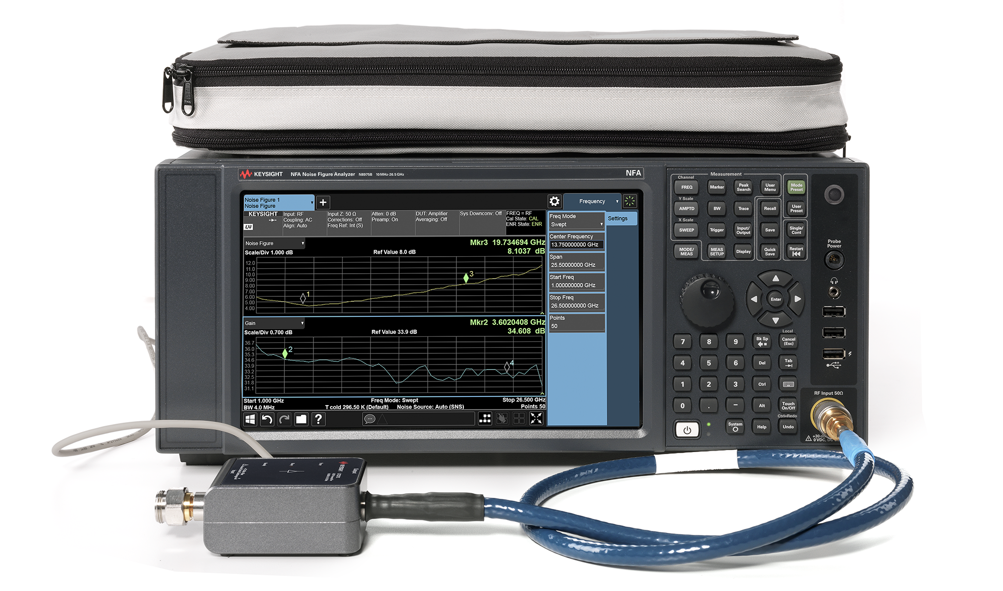
| 6 | Noise Figure Measurements | Keysight N8975B Noise Figure Analyzer | The N8975B high performance noise figure analyzer is designed to make fast, accurate and repeatable noise figure measurements. When paired with an SNS Series noise source and U7227 Series USB preamplifier the ENR data from the SNS and USB preamplifier data automatically downloads into the N8975B. |
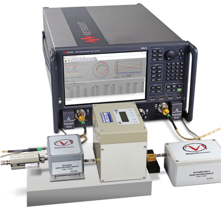
| 7 | Thermal Noise Measurements | Maury Microwave MT553A03 | Maury Microwave MT7553A03 (direct frequency to 26.5 GHz) is thermal noise measurement setup. |
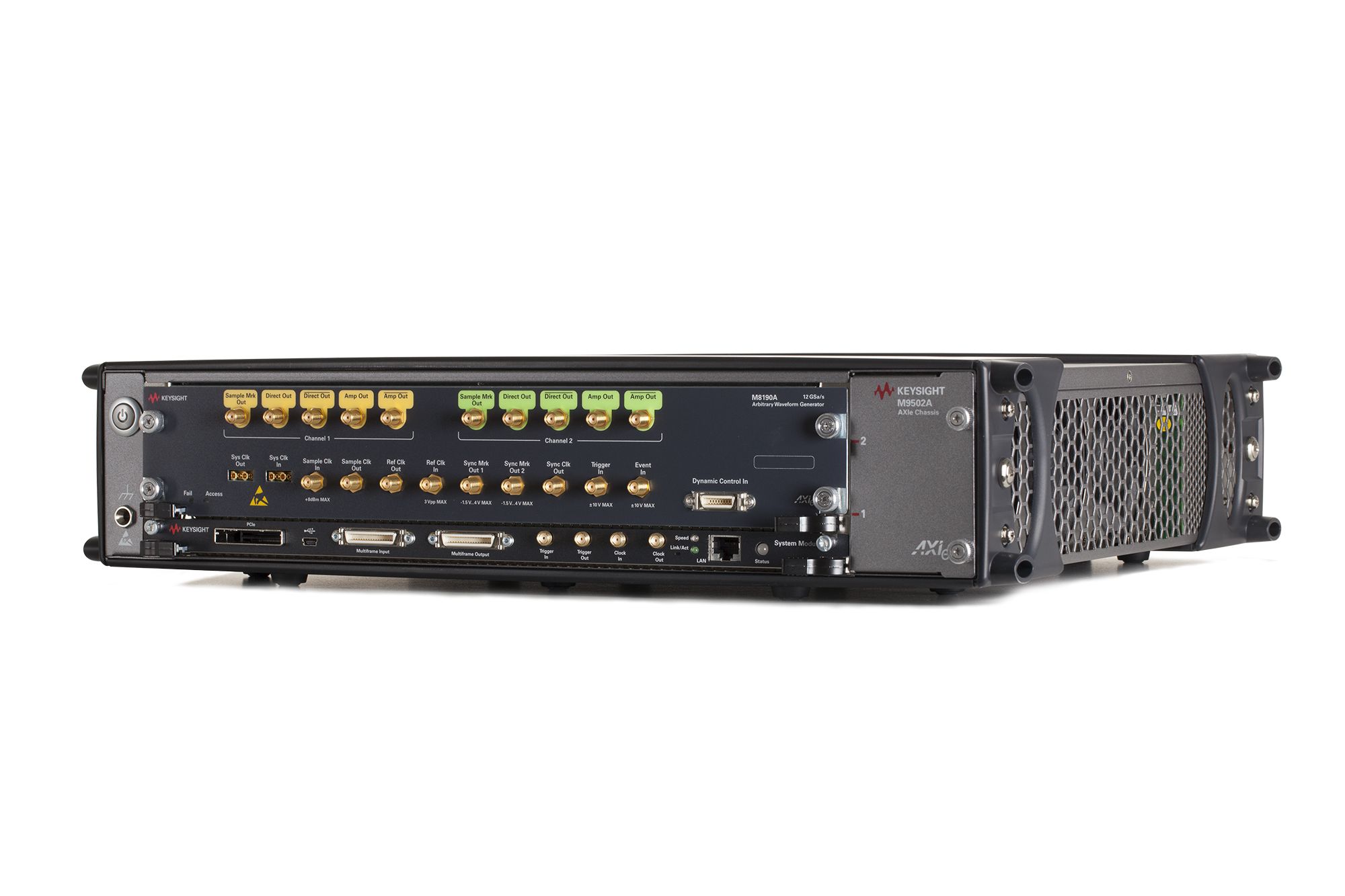
| 8 | Arbitrary Waveform Generator | Keysight M8190A AWG – 12 GSa/s | The Keysight M8190A is a high-performance ARBITRARY WAVEFORM GENERATOR (AWG) in the AXIe form factor, designed for demanding test environments such as radar, electronic warfare, satellite communications, and A/D converter validation. |
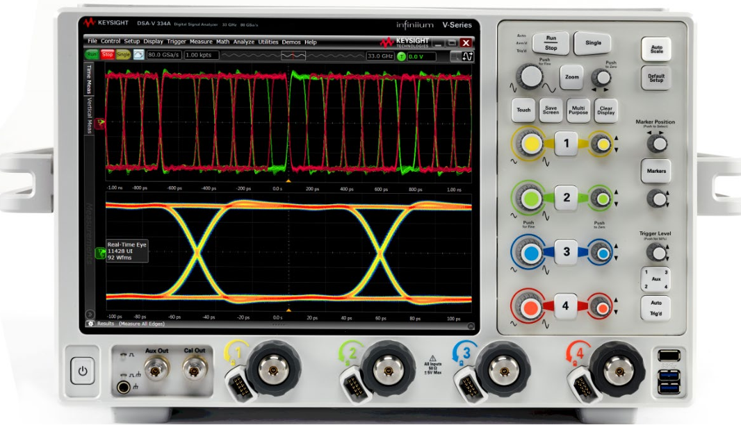
| 9 | Real Time Oscilloscope | Keysight DSOV084A | Infiniium V-Series oscilloscopes incorporate innovative technology designed to deliver superior measurements. Whether you are testing multiple high-speed serial lanes or a massive parallel bus, the new 12.5 Gb/s, exceptionally long 160-bit hardware serial trigger and fast 20 GSa/s digital channels will provide timely validation and debug.. |